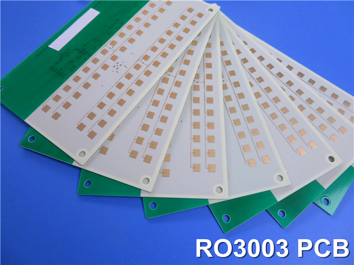
RO3003 PCB 4-Layer 2.4mm Thick: High-Frequency Ceramic-Filled PTFE Laminates for Automotive Radar and 5G mmWave Applications
1. Introduction of RO3003
Rogers RO3003 high-frequency laminates are ceramic-filled PTFE composites designed for commercial microwave and RF applications. These laminates provide excellent stability of the dielectric constant (Dk) across a range of temperatures and frequencies, effectively eliminating the step change in Dk commonly seen near room temperature in PTFE glass materials. This characteristic makes them ideal for applications such as automotive radar (77 GHz), advanced driver assistance systems (ADAS), and 5G wireless infrastructure (mmWave).
2. Features
Ceramic-filled PTFE composites from Rogers RO3003
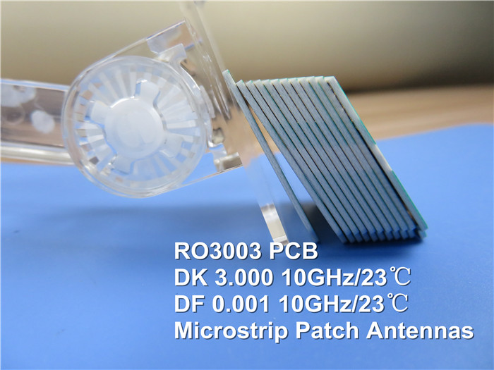
Dielectric constant of 3 ± 0.04 at 10 GHz/23°C
Dissipation factor of 0.001 at 10 GHz/23°C
Decomposition temperature (Td) greater than 500°C
Thermal conductivity of 0.5 W/mK
Moisture absorption of 0.04%
Coefficient of thermal expansion (from -55 to 288 °C): X-axis 17 ppm/°C, Y-axis 16 ppm/°C, Z-axis 25 ppm/°C
3. Benefits
Low dielectric loss, suitable for applications up to 77 GHz.
Excellent mechanical properties at varying temperatures, ensuring reliable stripline and multilayer board constructions.
Uniform mechanical properties across a range of dielectric constants, making it ideal for multilayer board designs and compatible with epoxy glass hybrid designs.
Stable dielectric constant with respect to temperature and frequency, perfect for bandpass filters, microstrip patch antennas, and voltage-controlled oscillators.
Low in-plane expansion coefficient that matches copper, enhancing the reliability of surface-mounted assemblies and stability in temperature-sensitive applications.
Economical laminate pricing suitable for volume manufacturing processes.
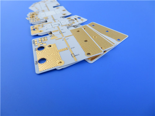
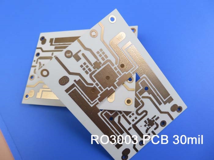
4. PCB Stackup: 4-layer Rigid PCB
Copper Layer 1: 35 µm
Rogers RO3003: 60 mil (1.524 mm)
Copper Layer 2: 35 µm
Prepreg RO4450F: 4 mil (0.101 mm)
Copper Layer 3: 35 µm
Rogers RO3003: 20 mil (0.508 mm)
Copper Layer 4: 35 µm
5. PCB Construction Details
Board dimensions: 190 mm x 90 mm (1 piece)
Minimum trace/space: 4/4 mils
Minimum hole size: 0.4 mm
Blind vias from inner layer 2 to the bottom layer, via filled and capped.
Finished board thickness: 2.4 mm
Finished copper weight for inner and outer layers: 1 oz (1.4 mils)
Via plating thickness: 20 µm
Surface finish: Immersion gold
Top silkscreen: Yellow
Bottom silkscreen: Green
Top solder mask: No
Bottom solder mask: Green
Countersunk holes required on the top layer at 90 degrees
100% electrical testing conducted prior to shipment
6. PCB Statistics
Components: 27
Total pads: 73
Through-hole pads: 47
Top SMT pads: 26
Bottom SMT pads: 0
Vias: 97
Nets: 4
7. Type of Artwork Supplied
Gerber RS-274-X
8. Accepted Standard
IPC-Class-2
9. Availability
Worldwide
10. Some Typical Applications
Automotive radar applications
Global positioning satellite antennas
Cellular telecommunications systems, including power amplifiers and antennas
Patch antennas for wireless communications
Direct broadcast satellites
Datalink on cable systems
Remote meter readers
Power backplanes
|
.jpg)
.jpg)
.jpg)